Guides / Grades
Choosing an ESD PEEK Grade for Wafer Handling Parts
October 13, 2026
Sources: manufacturer datasheets and published standards. See editorial standards.
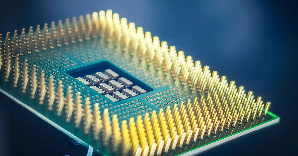
Unfilled PEEK is an excellent insulator, and that is a problem in a wafer fab. Plastic that holds charge attracts particles, and a sudden discharge can damage a device. Wafer handling parts therefore use a version of PEEK with a filler that lets charge bleed away at a controlled rate. Getting the resistance right, without adding particles or losing mechanical performance, is the real work, and it starts with the drawing.
Conductive, dissipative and insulative
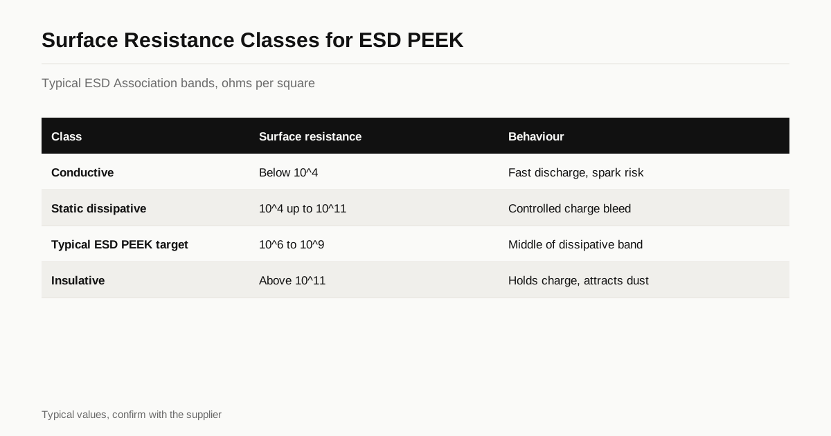
Electrostatic discharge standards divide materials by surface resistance. Typical bands, per the ESD Association classification, are:
| Class | Surface resistance, ohms per square | Behaviour |
|---|---|---|
| Conductive | Below 10 to the 4 | Charge flows away at once, spark risk |
| Static dissipative | 10 to the 4 up to 10 to the 11 | Charge bleeds away in a controlled way |
| Insulative | Above 10 to the 11 | Charge stays, particles attract |
Most ESD PEEK parts for wafer handling target the middle of the dissipative band, often 10 to the 6 to 10 to the 9 ohms per square. Too low and a charged wafer can discharge fast enough to harm a device. Too high and charge lingers. The number your tool needs comes from the equipment maker or the fab, so ask before choosing a grade.
Standard test methods exist for surface resistance and resistance to ground. Name the method, the electrode and the humidity on the drawing, because readings change with all three.
How PEEK is made dissipative
Three fillers are common.
Carbon fibre. Standard carbon filled PEEK is stiff and wear resistant, but its resistivity depends on how the fibres touch. It can swing from conductive to insulative across one part, and fibres can shed from the surface. It suits parts where a conductive path is acceptable and cleanliness is secondary.
Carbon powder. Fine carbon particles give a more uniform resistance and less shedding than fibre. The result is a black material with moderate stiffness and a narrower resistance window.
Carbon nanotubes. A small fraction of nanotubes forms a conductive network at low loading. These grades often show tighter resistance control, good mechanical properties and low particle release, so they are common in semiconductor handling. They cost more.
All three make the material black and reduce toughness compared with unfilled PEEK. See PEEK grades compared for how fillers change properties in general.
Cleanliness and particle control
A wafer handling part touches the wafer or sits next to it. Particles, ionic residue and outgassing all count.
- Particle shedding. Fibre filled grades can release fibres at cut edges and worn surfaces. Powder or nanotube grades shed less. Specify a surface finish and a cleaning method, and ask whether particle counts will be reported.
- Outgassing. PEEK is a low outgassing polymer, but fillers and processing aids can change that. The semiconductor outgassing guide explains what to ask.
- Ionic contamination. Some fillers add trace ions. For wafer contact surfaces, check supplier data on extractables.
- Cleaning and packing. Parts are washed and bagged in a controlled environment. See cleanroom packing.
Machining ESD grades
ESD PEEK machines much like carbon filled PEEK, with diamond coated or PCD tools for longer life. Three points affect results.
Resistance on the cut surface. Machining removes the stock skin, and the surface resistance on a cut face can differ from the skin. Measure the finished part, and say which surfaces matter.
Edge quality. Chipped edges release particles. Sharp tools, light finishing cuts and a deburring step reduce that.
Heat and stress. ESD grades hold stress like other PEEK, so annealing between roughing and finishing applies. See annealing PEEK parts.
Tolerance and flatness matter on wafer contact pads, end effectors and edge grips. A warped part loads a wafer unevenly, which can cause slip or a scratch. The wafer carrier specification guide covers flatness and surface finish for carriers.
Where ESD PEEK is used
Typical parts include wafer end effectors and pads, edge grip fingers, wafer carrier components, test sockets and probe card fixtures, alignment rings and chuck covers. The wider picture of semiconductor applications is in PEEK parts for semiconductor equipment, and test hardware in test sockets and probe card parts.
Testing and certifying resistance
Resistance is a number only when you say how it was measured. Surface resistance depends on electrode geometry, applied voltage, humidity and how long the part has been conditioned. Two labs can report different values on the same part if they use different methods.
A workable specification names five things:
- The test method, such as the ESD Association surface resistance method for solid materials.
- The electrode type and the force applied to the part.
- The test voltage, often 10 V or 100 V depending on the range.
- The conditioning, for example 24 hours at 12 percent relative humidity, since dissipative materials can read differently dry than humid.
- The locations on the part, such as the contact pad, the body and the mounting face.
Ask for a resistance reading on a finished part from each lot, or at least on witness coupons machined from the same bar. Stock suppliers publish the resistance range of the compound, and a lot certificate can confirm the figure, but machining changes the surface and a reading on the finished part is the one that counts for a wafer tool.
Common mistakes
Four mistakes recur on ESD PEEK orders.
Asking for conductive when dissipative is meant. A conductive part discharges too fast and can damage a device. Check the range with the tool maker.
Ignoring the skin. Stock surfaces and cut surfaces can read differently. Specify where the reading applies.
Mixing black grades. A standard black carbon filled PEEK, an ESD grade and a black pigmented PEEK all look the same. Lot labels and certificates prevent a mix-up, and the material verification guide explains how to check them.
Cleaning with the wrong fluid. A cleaning step that leaves a film can change surface resistance. Use the cleaning method agreed with the buyer, and test after cleaning.
Wear and surface life
An ESD surface can change with use. Wear exposes fresh material, rubbing against a wafer can polish the surface and cleaning fluids can change the top layer. Resistance readings taken at purchase therefore drift over the life of a part. Ask the tool maker how often resistance is rechecked in service, and whether a replacement interval is set by wear or by a resistance reading. For contact pads that touch wafers every cycle, replace on a schedule, not on failure.
Dissipative grades sit in the electrical step of our guide to PEEK grade selection.
What to put on the RFQ
State the resistance range, the test method and the humidity, the particle and cleanliness requirement, the grade or filler type and the surface finish on contact areas. Say whether the supplier must report a resistance measurement on each lot. Send the drawing and we match you with up to three shops that machine ESD plastics, with a reply within 24 business hours.
See also: how ESD PEEK is tested, from surface resistance to resistivity methods.
See also: ESD and static-dissipative PEEK, the grade reference page with published ranges by maker.
Frequently asked questions
What surface resistance should an ESD PEEK part have?
Static dissipative parts usually sit between 10 to the 6 and 10 to the 9 ohms per square, which discharges a charge in a controlled way. The range your tool needs is set by the equipment maker or the fab, so ask for the number before choosing a grade.
Does machining change the resistance of ESD PEEK?
It can. The surface skin of stock sometimes reads differently from the bulk, and a cut surface may read higher or lower than a moulded or extruded skin. Measure the finished part, not the stock, and say where on the part the measurement applies.
Is carbon fibre filled PEEK the same as ESD PEEK?
Not necessarily. Standard carbon filled PEEK is often conductive in places and its resistance varies widely. ESD grades use a controlled filler, such as carbon powder or nanotubes, to hold resistance inside a narrow dissipative window and to shed fewer particles.
Need a quote for this part?
Send the drawing. We match you with up to 3 shops that cut your PEEK grade and reply within 24 business hours.
Get matched with a PEEK shop